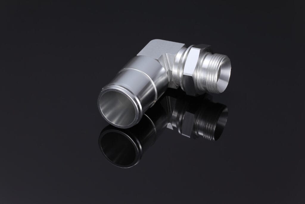
Precision Manufacturing Case Study: High-Precision Stainless Steel Valve Body for Semiconductor Equipment

Project Background

Project Background: Conquering Ultra-Clean and Micron-Level Precision Challenges

In early 2025, as a leading global semiconductor equipment manufacturer was upgrading its wafer handling system, their engineering team encountered persistent quality issues with their high-purity gas control valve bodies. Existing suppliers’ 316L stainless steel components showed microscopic burrs and inconsistent surface finishes, resulting in vacuum seal failures and particle contamination risks—an unacceptable threat in semiconductor manufacturing.

Having learned of our specialized expertise in semiconductor-grade stainless steel precision machining (particularly our vacuum chamber components for etching equipment), their Asia Pacific Procurement Director, James Wong, contacted our Technical Director, Mr. Li. Facing a tight installation deadline for their new production line, they urgently needed 30 ultra-precision valve body assemblies for cleanroom testing, particle analysis, and lifecycle validation.


Key Technical Challenges

Complex Flow Channel Machining

Intersecting deep channels requiring absolute burr-free and uniform internal surfaces

Micron-Level Surface Integrity

Zero microscopic defects permitted on sealing surfaces

Cleanliness Control

Strict avoidance of carbon steel contamination throughout machining

Accelerated Timeline

 15 days to complete material prep, 5-axis machining, deburring, electropolishing, full inspection, and clean packaging

Our Solution: Semiconductor-Grade Precision Manufacturing System

Material Selection & Process Planning

We selected vacuum-melted 316L stainless steel bar stock, with full traceability and material certifications, including corrosion performance and non-metallic inclusion reports for each batch.

Collaborative Process Innovation

Senior Process Engineer Wang Gong tackled the intersecting channel burr challenge with a customized approach: Implemented combined drilling-milling strategies to ensure seamless channel transitions Deployed custom PCD (polycrystalline diamond) tools for critical finishing operations

Developed non-contact inspection fixtures for verification

During simulation, a stress deformation risk was identified between sealing surfaces and mounting flanges. A virtual emergency meeting was convened with the client's mechanical team in Germany, resulting in a revised machining sequence—completing sealing surface finishing before side-hole processing—which enhanced dimensional stability without compromising design intent.

Precision Machining Execution

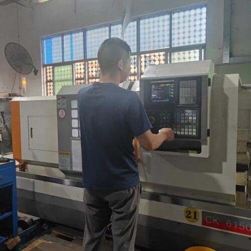
First-article inspection confirmed sealing surface flatness within 0.004mm. However, micro-burrs were detected at channel intersections. Our team responded immediately: Revised tool paths and cutting parameters in real-time Implemented high-pressure directional deburring technology Incorporated an additional electrochemical deburring (ECM) step These adjustments ensured subsequent components met all flow channel specifications without exception.

Semiconductor-Grade Surface Treatment

All components underwent processing in Class 1000 cleanroom conditions: Three-stage ultrasonic cleaning Precision electropolishing for mirror-grade finish Passivation treatment forming consistent protective layer Nitrogen purging and sealing The entire process adhered to semiconductor equipment packaging protocols with continuous particle monitoring.

Comprehensive Quality Traceability

Each component underwent CMM and white light scanning inspection. One unit showed a flow channel aperture deviation of 0.003mm beyond tolerance. Our quality team: Immediately activated non-conformance protocols Provided client with detailed deviation analysis within hours Isolated the component and initiated re-machining Approved units were packaged using dual-layer clean packaging with integrated particle test reports, shipped via dedicated logistics channels.

George
George— James Wong, Procurement Director
"The assemblies arrived on the morning of day 15 in perfect condition. All seal tests passed on first attempt, and particle counts were significantly better than expected. Your team's solution for the flow channel burr issue was particularly impressive—it eliminated a critical contamination risk we've struggled with for months. We are proceeding with an initial batch order for 200 units."

Future Collaboration

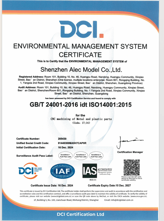
This project transitioned into a recurring monthly order, with batch deliveries every two weeks. We’ve also helped the client set up batch traceability templates and inspection routines compatible with their CE and ISO9001 requirements.
Future projects include development of similar modules for a new inverter control platform.

After three successful deliveries with no major quality concerns, client satisfaction remains strong. We’ve since been invited to support two upcoming platform projects, with technical discussions scheduled for next quarter—marking the start of a deeper, long-term collaboration.

Project Insight: Precision × Cleanliness × Traceability

This project exemplifies how integrated material science, process innovation, and quality systems meet semiconductor manufacturing’s unique demands. The seamless transition from 30 validation units to sustained production underscores our capacity to deliver technical excellence for high-stakes manufacturing applications.

Facebook
Twitter
LinkedIn